- 您现在的位置:买卖IC网 > Sheet目录337 > LH28F160S3HNS-TV (Sharp Microelectronics)IC FLASH 16MBIT 100NS 56SSOP
�� �
�
�LHF16KTV�
�3�
�Internal� V� CC� and� V� PP�
�1� INTRODUCTION�
�This� datasheet� contains� LH28F160S3HNS-TV�
�specifications.� Section� 1� provides� a� flash� memory�
�overview.� Sections� 2,� 3,� 4,� and� 5� describe� the�
�memory� organization� and� functionality.� Section� 6�
�covers� electrical� specifications.�
�1.1� Product� Overview�
�The� LH28F160S3HNS-TV� is� a� high-performance�
�16M-bit� Smart� 3� Flash� memory� organized� as�
�2MBx8/1MBx16.� The� 2MB� of� data� is� arranged� in�
�thirty-two� 64K-byte� blocks� which� are� individually�
�erasable,� lockable,� and� unlockable� in-system.� The�
�memory� map� is� shown� in� Figure� 3.�
�Smart� 3� technology� provides� a� choice� of� V� CC� and�
�V� PP� combinations,� as� shown� in� Table� 1,� to� meet�
�system� performance� and� power� expectations.� 2.7V�
�V� CC� consumes� approximately� one-fifth� the� power� of�
�5V� V� CC� .� V� PP� at� 2.7V,� 3.3V� and� 5V� eliminates� the�
�need� for� a� separate� 12V� converter,� while� V� PP� =5V�
�maximizes� erase� and� write� performance.� In� addition�
�to� flexible� erase� and� program� voltages,� the� dedicated�
�V� PP� pin� gives� complete� data� protection� when�
�V� PP� ≤� V� PPLK� .�
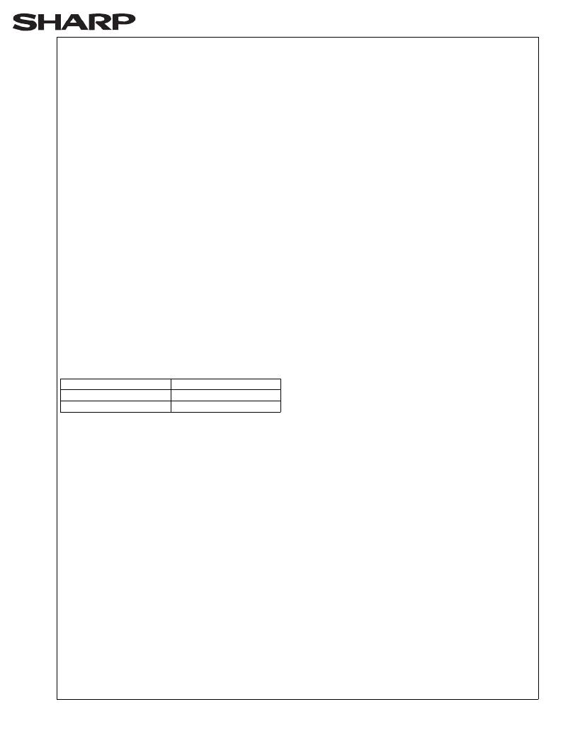
�Table� 1.� V� CC� and� V� PP� Voltage� Combinations�
�Offered� by� Smart� 3� Technology�
�V� CC� Voltage� V� PP� Voltage�
�2.7V� 2.7V,� 3.3V,� 5V�
�3.3V� 3.3V,� 5V�
�detection� Circuitry�
�automatically� configures� the� device� for� optimized�
�read� and� write� operations.�
�A� Command� User� Interface� (CUI)� serves� as� the�
�interface� between� the� system� processor� and� internal�
�operation� of� the� device.� A� valid� command� sequence�
�written� to� the� CUI� initiates� device� automation.� An�
�internal� Write� State� Machine� (WSM)� automatically�
�executes� the� algorithms� and� timings� necessary� for�
�block� erase,� full� chip� erase,� (multi)� word/byte� write�
�and� block� lock-bit� configuration� operations.�
�A� block� erase� operation� erases� one� of� the� device’s�
�64K-byte� blocks� typically� within� 0.41s� (3.3V� V� CC� ,� 5V�
�V� PP� )� independent� of� other� blocks.� Each� block� can� be�
�independently� erased� 100,000� times� (3.2� million�
�block� erases� per� device).� Block� erase� suspend� mode�
�allows� system� software� to� suspend� block� erase� to�
�read� or� write� data� from� any� other� block.�
�A� word/byte� write� is� performed� in� byte� increments�
�typically� within� 12.95μs� (3.3V� V� CC� ,� 5V� V� PP� ).� A� multi�
�word/byte� write� has� high� speed� write� performance� of�
�write� suspend� mode� enables� the� system� to� read� data�
�or� execute� code� from� any� other� flash� memory� array�
�location.�
�Individual� block� locking� uses� a� combination� of� bits�
�and� WP#,� Thirty-two� block� lock-bits,� to� lock� and�
�unlock� blocks.� Block� lock-bits� gate� block� erase,� full�
�chip� erase� and� (multi)� word/byte� write� operations.�
�Block� lock-bit� configuration� operations� (Set� Block�
�Lock-Bit� and� Clear� Block� Lock-Bits� commands)� set�
�and� cleared� block� lock-bits.�
�The� status� register� indicates� when� the� WSM’s� block�
�erase,� full� chip� erase,� (multi)� word/byte� write� or� block�
�lock-bit� configuration� operation� is� finished.�
�The� STS� output� gives� an� additional� indicator� of� WSM�
�activity� by� providing� both� a� hardware� signal� of� status�
�(versus� software� polling)� and� status� masking�
�(interrupt� masking� for� background� block� erase,� for�
�example).� Status� polling� using� STS� minimizes� both�
�CPU� overhead� and� system� power� consumption.� STS�
�pin� can� be� configured� to� different� states� using� the�
�Configuration� command.� The� STS� pin� defaults� to�
�RY/BY#� operation.� When� low,� STS� indicates� that� the�
�WSM� is� performing� a� block� erase,� full� chip� erase,�
�(multi)� word/byte� write� or� block� lock-bit� configuration.�
�STS-High� Z� indicates� that� the� WSM� is� ready� for� a�
�new� command,� block� erase� is� suspended� and� (multi)�
�word/byte� write� are� inactive,� (multi)� word/byte� write�
�are� suspended,� or� the� device� is� in� deep� power-down�
�mode.� The� other� 3� alternate� configurations� are� all�
�pulse� mode� for� use� as� a� system� interrupt.�
�The� access� time� is� 100ns� (t� AVQV� )� over� the� extended�
�temperature� range� (-40°C� to� +85°C)� and� V� CC� supply�
�voltage� range� of� 3.0V-3.6V.� At� lower� V� CC� voltage,� the�
�access� time� is� 120ns� (2.7V-3.6V).�
�The� Automatic� Power� Savings� (APS)� feature�
�substantially� reduces� active� current� when� the� device�
�is� in� static� mode� (addresses� not� switching).� In� APS�
�mode,� the� typical� I� CCR� current� is� 3� mA� at� 3.3V� V� CC� .�
�When� either� CE� 0� #� or� CE� 1� #,� and� RP#� pins� are� at� V� CC� ,�
�the� I� CC� CMOS� standby� mode� is� enabled.� When� the�
�RP#� pin� is� at� GND,� deep� power-down� mode� is�
�enabled� which� minimizes� power� consumption� and�
�provides� write� protection� during� reset.� A� reset� time�
�(t� PHQV� )� is� required� from� RP#� switching� high� until�
�outputs� are� valid.� Likewise,� the� device� has� a� wake�
�time� (t� PHEL� )� from� RP#-high� until� writes� to� the� CUI� are�
�recognized.� With� RP#� at� GND,� the� WSM� is� reset� and�
�the� status� register� is� cleared.�
�The� device� is� available� in� 56-Lead� SSOP� (Shrink�
�Small� Outline� Package).� Pinout� is� shown� in� Figure� 2.�
�2.7μs/byte� (3.3V� V� CC� ,� 5V� V� PP� ).� (Multi)� Word/byte�
�Rev.� 2.0�
�发布紧急采购,3分钟左右您将得到回复。
相关PDF资料
LH28F160S5HNS-S1
IC FLASH 16MBIT 70NS 56SSOP
LH28F320S3HNS-ZM
IC FLASH 32MBIT 110NS 56SSOP
LH28F320SKTD-ZR
IC FLASH 32MBIT 70NS 48TSOP
LHF00L28
IC FLASH 16MBIT 70NS 48TSOP
LPM409 CHASSIS
STNRD 4SLOT CHASSIS W/INPUT LEAD
LS15RB1201J04
POE SPLITTER 10.8W 12V @0.9A
LT1932ES6#TRMPBF
IC LED DRIVR WHITE BCKLGT TSOT-6
LT1937ES5#TRMPBF
IC LED DRIVR WHITE BCKLGT TSOT-5
相关代理商/技术参数
LH28F160S3HR-L10
制造商:未知厂家 制造商全称:未知厂家 功能描述:x8/x16 Flash EEPROM
LH28F160S3HR-L13
制造商:未知厂家 制造商全称:未知厂家 功能描述:EEPROM|FLASH|1MX16/2MX8|CMOS|TSSOP|56PIN|PLASTIC
LH28F160S3HT-L10
制造商:Sharp Microelectronics Corporation 功能描述:NOR Flash Parallel 3V 16Mbit 2M/1M x 8bit/16bit 100ns 56-Pin TSOP
LH28F160S3HT-L10A
功能描述:IC FLASH 16MBIT 100NS 56TSOP RoHS:否 类别:集成电路 (IC) >> 存储器 系列:- 标准包装:96 系列:- 格式 - 存储器:闪存 存储器类型:FLASH 存储容量:16M(2M x 8,1M x 16) 速度:70ns 接口:并联 电源电压:2.65 V ~ 3.6 V 工作温度:-40°C ~ 85°C 封装/外壳:48-TFSOP(0.724",18.40mm 宽) 供应商设备封装:48-TSOP 包装:托盘
LH28F160S3HT-L13
制造商:未知厂家 制造商全称:未知厂家 功能描述:EEPROM|FLASH|1MX16/2MX8|CMOS|TSSOP|56PIN|PLASTIC
LH28F160S3HT-L75A
制造商:Sharp Microelectronics Corporation 功能描述:
LH28F160S3HT-TF
功能描述:IC FLASH 16MBIT 100NS 56TSOP RoHS:是 类别:集成电路 (IC) >> 存储器 系列:- 标准包装:1 系列:- 格式 - 存储器:RAM 存储器类型:SDRAM 存储容量:256M(8Mx32) 速度:143MHz 接口:并联 电源电压:3 V ~ 3.6 V 工作温度:-40°C ~ 85°C 封装/外壳:90-VFBGA 供应商设备封装:90-VFBGA(8x13) 包装:托盘 其它名称:Q2841869
LH28F160S3-L10
制造商:SHARP 制造商全称:Sharp Electrionic Components 功能描述:16-MBIT(2MBx8/1MBx16) Smart 3 Flash MEMORY